Product Center
About Us
Ginkgo Micro Semiconductor has been deeply involved in the semiconductor power device industry for many years, focusing on the core field of MOSFETs. It integrates research and development, production, testing, sales, and application services, and is a highly competitive MOSFET manufacturer and application solution provider in China.
We adhere to the concept of "technology led, quality-oriented, and customer-oriented", and have formed a research and application team composed of senior engineers in the industry. We have advanced production lines and precision testing equipment, and strictly control the quality from chip design, wafer manufacturing to packaging testing, ensuring that every product meets industry standards and customer needs.
As MOSFET application experts, we not only provide standardized products, but also offer customized full process services such as device selection, circuit design, and technical debugging based on customers' specific application scenarios. We solve various technical problems encountered by customers in the application process, help customers shorten research and development cycles, reduce production costs, and enhance product competitiveness.
We always take technological innovation as the core driving force, continuously invest in research and development resources, track cutting-edge technologies in the industry, optimize product performance, and promote the deep application of MOSFET technology in various fields.

Our Advantages
Advanced equipment
The manufacturing equipment mainly consists of imported AMS equipment, with over 70% being fully automated equipment.
Advanced process
Having multiple technical patents and constantly innovating technologies
Standard procedure
The company implements standardized production processes, with each production link closely connected to ensure controllable and orderly production of products.
EU ROHS standard
The factory has passed ISO quality system certification and its performance meets the EU ROHS standard.
Application
News

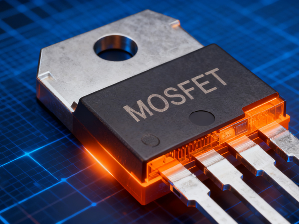
The full name of MOSFET is metal oxide semiconductor field-effect transistor

Its core consists of four key components: source (current inlet), drain (current outlet), gate (voltage control terminal), and semiconductor substrate. The gate and channel are completely isolated by a thin layer of silicon dioxide insulation.

Learn more


Technical characteristics and applicable scenarios of different types of MOSFETs

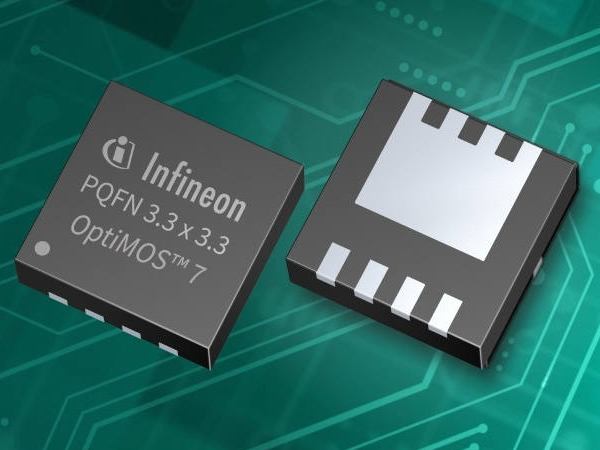
The technical characteristics and applicable scenarios of different types of MOSFETs vary significantly. The following is a summary of the mainstream classification dimensions:Divided by channel typeN-channel MOSFETTechnical features: The electron mobility is much higher than that of holes, and the conduction resistance is lower and the switching speed is faster under the same size, making it the mainstream choice in the current market; The conduction condition is that the gate source voltage VGS is greater than the positive threshold voltage, and the driving logic is simple.Applicable scenarios: Low voltage and high current DC-DC converters, industrial motor drives, vehicle power supplies, high-power fast charging, and most other power switch scenarios. For example, the SL18N20 with 200V/18A specifications can be directly adapted to mainstream PWM controllers without the need for additional level conversion circuits.P-channel MOSFETTechnical features: Using holes as carriers, with a transconductance lower than that of N-channel devices of the same specifications, a higher absolute threshold voltage, and a gate source voltage VGS lower than the negative threshold for conduction; Naturally adapted to high-end driving scenarios, without the need for complex bootstrap circuits.Applicable scenarios: Power path management for battery powered equipment, high-end load switches, anti reverse protection circuits, especially suitable for simple drive architectures where the source is directly connected to VCC.

Learn more


How to choose the appropriate MOSFET type

The selection of suitable MOSFETs is based on the core constraints of the application scenario, and is screened layer by layer according to the steps of "determining the technical route first, then sticking to key parameters, and finally verifying reliability and supply chain", to avoid performance waste or reliability risks caused by blindly pursuing extreme parameters.

Learn more


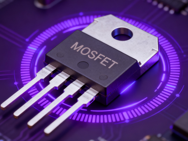
MOSFET is a widely used field-effect device in the current semiconductor field

MOSFET is a widely used field-effect device in the current semiconductor field, with core structural characteristics:It consists of a three-layer core structure consisting of a metal gate, an oxide insulating dielectric, and a semiconductor substrate. The channel conduction state is controlled by gate voltage to achieve current switching control.

Learn more


Contact Us

  • 17374646018
    E-mail: huqinfu@ginkgomos.com
    Address: 2nd Floor, Honghai Central Asia Silicon Valley Building, Hongxing Community, Songgang Street, Bao'an District, Shenzhen

    Follow the latest information

CopyRight © 2026 Shenzhen Ginkgo Micro Semiconductor Co., Ltd. All Rights Reserved.    粤ICP备2026030774号